

EDA tools for PCB designs is a jungle. There are a lot of options to choose from, and the compatibility between different tools is generally poor – even for tools from the same vendor. We have seen an increase in porting requests from existing and new customers. Relevant designs that have been captured in EDA tools that are no longer suitable.
Converting between tools is never as straight forward as promised by EDA vendors – there are many porting tools available, but they almost always fall short. Importing a gerber file is simple enough – but the connections, part databases and physical design ruleset that served as the foundation to create that layout is another story.
This blog post briefly discusses the purpose of a schematic and describes a method that ShortLink uses to compare netlists, one of the most important purposes of the schematic.
What’s in a schematic?
The schematic can be used for different purposes depending on the design paradigm used by a particular company. It’s typically a combination of the following:
- Give a graphical understanding of the design. An engineer can understand how a board works by studying the schematic. This information is typically retained pretty well during a schematic import.
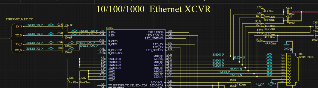
- Specify connectivity – allowing the generation of a Netlist. The netlist defines all points that should be connected by copper, and is provided to the layout tool. This can be problematic durign import and is described further in this blog post.
- Specify the electrical components used in the design. The components used in the schematic typically correspond to layout footprints used by the layout tool. This will be the subject of a later blog post. Note: I use the word “component” loosely here – a lot can be be said about design parts, purchasing parts, components, symbols, footprints, mechanical parts, BOMs etc.
- Specify netclasses. A schematic can include information on which nets are sensitive, need to handle a certain amount of current, balances pairs, impedance and so on. This is typically entered manually.
- Provide metadata such as design engineer, design date, revision. During import, this is handled manually on a case-by-case basis: should the converted PCB project be managed by ShortLink or the customer?
Copper Connectivity
It is vital that the connectivity described netlist is identical between the original schematic and the imported version. Our experience is that some manual adjustments of the imported schematic are typically necessary to achieve this. During import the schematic can be interpreted differently in different tools (3-way and 4-way junctions, global nets, case sensitivity).
Thankfully, it is relatively straight forward to verify when the connectivity is identical: generate a netlist in the original schematic, and compare it with the netlist in the new tool. The problem is that the netlist formats are usually not directly comparable, and net names can change as part of the porting process.
To combat this, we have developed a small python script that generates netlists that can then be compared. It it designed for the PADS netlist file format, but it can easily be expanded to support other formats as well. We have chosen to work with PADS since many tools support them (for example Eagle, Altium, PADS..).
The script parses a PADS netlist, orders all the nets by connected nodes and creates an output file with the sorted netlist. By running the tool on two netlists, the two output files can be compared even if the order of the nets or the names of the nets are different: the intention is to compare the connected nodes.
By using the excellent diff tool Eskil , it is also possible to use some clever regexp pre-processing to further reduce false errors (e.g. ignoring the order of pin 1 and 2 of a resistor).
The python script is open source, license free and available at our github page. Please let us know if you find it useful!
Netlist Diff in Eskil
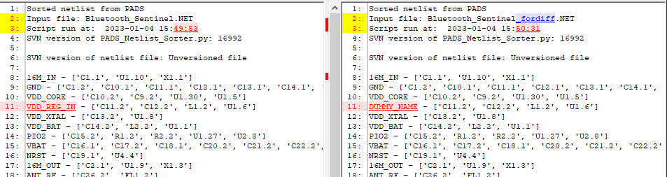
The image shows how a typical diff can look in Eskil. We see that the net VDD_REG_IN has been renamed to DUMMY_NAME, but since the script sorts by connectivity and not net name it’s easy to see that the netlists are equivalent.
Let us convert your design to Altium Designer
We have a detailed method at ShortLink that we use when converting PCB projects from other tools to our Altium environment. We get requests from many tools, most commonly Eagle and CadInt. We can of course make adjustments (e.g. replace EOL components) as part of the porting process. The method can be adjusted depending on your needs.
Please Contact us if you need help converting PCB projects between EDA tools!